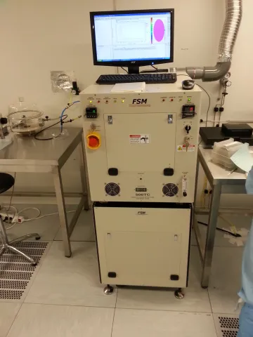
Thin Film Stress Measurement System (FSM 500TC)
FSM 500 TC
Stress measurement as function of temperature up to 500°C
Contact :
Etienne Herth
Bâtiment TEMIS Sciences, bureau N3
03 63 08 24 70 (Office)
03 63 08 21 04 (Cleanroom)
Etienne.herth [at] femto-st.fr (Etienne[dot]herth[at]femto-st[dot]fr)
Localization :
Cleanroom TEMIS
Overview :
Mechanical properties of materials used in microelectromechanical system (MEMS) and in a micro-fabrication process, are of fundamental importance. Particularly, residual stress in deposited film always exists when a thin layer is used in device micro-fabrication. This residual stress is typically thought of as being composed of two components: intrinsic and extrinsic. Intrinsic stresses are typically associated with growth process deposition. Extrinsic stresses are a result of external influences after deposition such as temperature change in the presence of mismatched coefficients of thermal expansion. Residual and thermal stresses additionally cause deformation in the normally planar substrate, altering the anticipated static and dynamic response of devices. Under high stress conditions devices may even become inoperable. As a result, during microfabrication stresses should be minimized for optimum operation of a MEMS device. Thus, it is necessary to determine, and later control, film stress in MEMS-MOEMS for various purposes such as guarantying structural integrity.
DESCRIPTION and SPECIFICATION :
- Stress range: 1 x 10⁷ to 4 x 10¹⁰ dynes/cm2 (Provided that the wafer curvature change before and after processing is greater than 1micron (bow height) for a 170mm scan line)
- Wafer sizes: 200mm or smaller
- Scan range: Up to 170mm
- Scan line: Single scan line at any wafer orientation
- Mapping: Multi scan line mapping by manually rotating wafers. Max of 6 line mapping with 30 deg between each line
- Repeatability: 1.0% (1 sigma) of average value using 5000A W wafer, measured 30X. (Ambient temperature)
- Results Report: Film Stress, Radius, Wafer bow Height, Temperature, Date and Time
- Laser type: Dual wavelength, 780nm and 650nm laser diodes