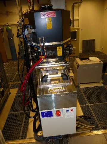
Deep Reactive Ion Etching Silicon (RAPIER SPTS)
Deep reactive Ion Etching Silicon (RAPIER SPTS)
Contact :
Djaffar BELHARET
TEMIS Sciences Building - Office N1-22
03 81 66 55 83 (Office)
03 63 08 23 74 (Dry Etching Area)
djaffar.belharet [at] femto-st.fr (djaffar[dot]belharet[at]femto-st[dot]fr)
Location :
TEMIS cleanroom
Dry Etching Area
Principle :
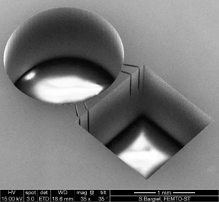
Silicon can be etched in an anisotropic (or isotropic) and dry way with
the technology called “deep RIE�?. This method combines deposition and
etching plasma assisted processes. While the silicon is etched, the
process enables to deposit a fluorinated component on the pattern walls
in order to passivate them. Etching-deposition cycles with given gases
and time enable to etch deeply and anisotropically the silicon
independently of its orientation.
Technical specifications :
- ICP source power : 5.5 kW RF
- Bias source power : 1.5 kW RF
- Electrostatic clamping with cooled wafer holder (0 to 40°C)
- Available gas : SF6, C4F8, Ar, He, N2 and O2
- Wafer size : pieces up to 4 inch
- Real-time endpoint detection system (Claritas)
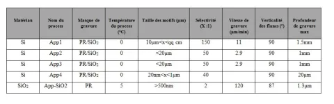
Etched materials :
This machine is only dedicated to the silicon and silica (<1µm) etching.
Table of etching performances :
Achieved results :