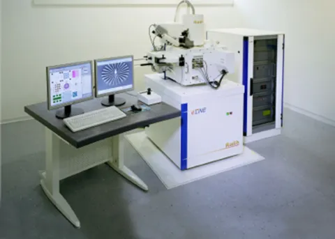
Electron beam lithography Raith E_Line
Electron beam lithography
Raith E_Line
Contact :
Roland SALUT
TEMIS Sciences Building - Office N2-28
03 63 08 21 07 (Office)
03 63 08 21 11 (Ebeam lithography Room)
roland.salut [at] femto-st.fr (roland[dot]salut[at]femto-st[dot]fr)
Location:
TEMIS cleanroom
Lithography area
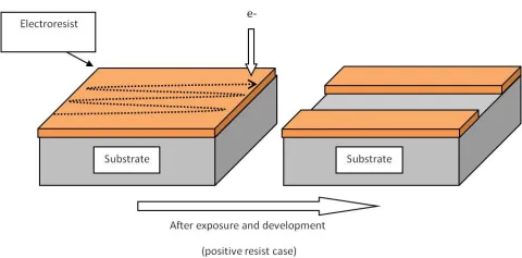
Principle :
An electron-beam resist is spin-coated on the substrate. Thanks to the Raith E_Line system, this resist is exposed to a high energy electron beam according to a pattern previously designed in a gdsii format. After development in an appropriate solution, the exposed resist is removed (in the positive resist case).
Technical characteristics :
- Filament : Schottky TFE
- Stage displacement : 100mm x 100mm x 30mm
- Spot size : <2nm @ 20keV
- Curent range : 5pA – 20nA
- Curent density : > 7500 A/cm²
- Curent stability : <0 .5%/h
- Detectors : In Lens, Everhart Thornley
- Minimum line width : 20nm
- Stitching accuracy : 60nm (mean 3 sigma)
- Layer to layer adjustment accuracy : 40nm (mean 3 sigma)
- Sample size : from chip to 4 inch wafers
- File format : GDSII
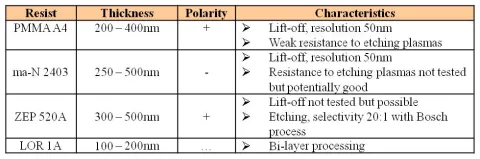
Available electron-beam resists:
The available resists are:
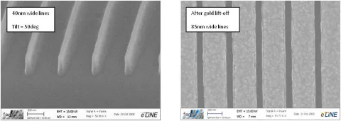
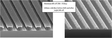
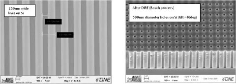
Achieved results :
PMMA A4
ma-N 2403
ZEP 520A