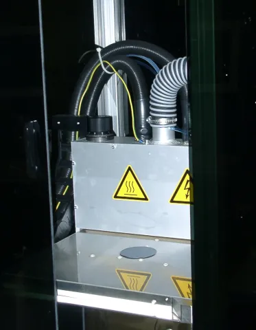
Nanoprep NP12
Surface activation by plasma
Nanoprep NP12
Contact :
Sylwester BARGIEL
TEMIS Sciences Building
03 81 66 63 02 (Office)
sylwester.bargiel [at] femto-st.fr (sylwester[dot]bargiel[at]femto-st[dot]fr)
Location :
TEMIS cleanroom
Wafer Bonding Area
Principle :
The plasma activation is based on the principle of discharge by dielectric barrier: the discharge is conducted between two electrodes separated by a gas space which is ionized by applying a voltage of a few kilovolts. To avoid the formation of an electric arc, which would lead to a very high degradation of the material, a solid electrical insulator (ceramic) is introduced between the electrodes.
The plasma discharge is limited to the electrode surfaces, a displacement of these surfaces is therefore necessary to treat all the entire wafer.
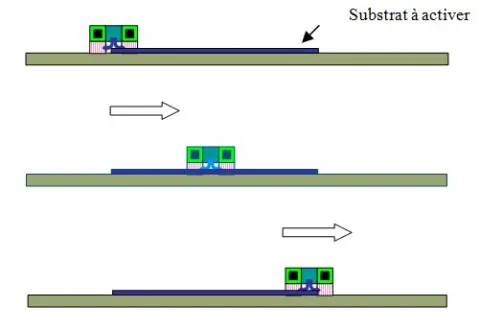
The plasma treatment induces a structural change of the surfaces by the formation of free radicals. The main effect is an increase of the surface tension: a hydrophilic surface is obtained.
Technical specifications :
- Very fast process (about 5s)
- 2 gas lines : N2, O2 (or Ar) depending on the surface to activate
- Substrate thickness : 1.5mm max
- Distance between wafer and electrodes to adjust to obtain a homogeneous and effective plasma
- Source power : 200W to 800W
- Scanning speed : 10 to 100mm/s
- Gas flow : up to 100 slm
Example of use :
The plasma activation allows, for example, to obtain a strong weld from 400°C by direct bonding while a temperature of 1100°C is needed without it. It can also be used before a photoresit coating to obtain a better adhesion and a better uniformity.